Tata teams with Genesys to boost enterprise engagement with enhanced InstaCC Platform
Logicalis adds Q Associates to bolster data management
HS2 sets aside £9.5m to cover cost of IR35 non-compliance
ASRock Industrial NUC BOX-1260P and 4X4 BOX-5800U Review: Alder Lake-P and Cezanne UCFF Faceoff
The past few years have seen Intel and AMD delivering new processors in a staggered manner. In the sub-45W category, Intel’s incumbency has allowed it to deliver products for both the notebook and ultra-compact form factor (UCFF) within a few months of each other. On the other hand, AMD’s focus has been on the high-margin notebook market, with the chips filtering down to the desktop market a year or so down the road. In this context, AMD’s Cezanne (most SKUs based on the Zen 3 microarchitecture) and Intel’s Tiger Lake went head-to-head last year in the notebook market, while Rembrandt (based on Zen3+) and Alder Lake-P are tussling it out this year. In the desktop space, Cezanne-based mini-PCs started making an appearance a few months back, coinciding with the first wave of Alder Lake-P systems. ASRock Industrial launched the NUC BOX-1200 series (Alder Lake-P) and the 4X4 BOX-5000 series (Cezanne) within a few weeks of each other. The company sent over the flagship models in both lineups for review, giving us a chance to evaluate the performance and value proposition of the NUC BOX-1260P and 4X4 BOX-5800U. Read on to find out how Alder Lake-P and Cezanne stack up against each other in the mini-PC space, and a look into what helps ASRock Industrial introduce mini-PCs based on the latest processors well ahead of its competitors.
<div>SK hynix Announces 238 Layer NAND – Mass Production To Start In H1’2023</div>

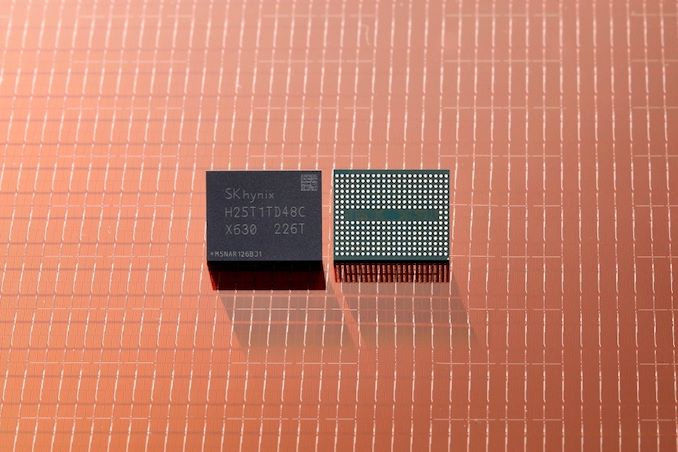
As the 2022 Flash Memory Summit continues, SK hynix is the latest vendor to announce their next generation of NAND flash memory at the show. Showcasing for the first time the company’s forthcoming 238 layer TLC NAND, which promises both improved density/capacity and improved bandwidth. At 238 layers, SK hynix has, at least for the moment, secured bragging rights for the greatest number of layers in a TLC NAND die – though with mass production not set to begin until 2023, it’s going to be a while until the company’s newest NAND shows up in retail products.
Following closely on the heels of Micron’s 232L TLC NAND announcement last week, SK hynix is upping the ante ever so slightly with a 238 layer design. Though the difference in layer counts is largely inconsequential when you’re talking about NAND dies with 200+ layers to begin with, in the highly competitive flash memory industry it gives SK hynix bragging rights on layer counts, breaking the previous stalemate between them, Samsung, and Micron at 176L.
From a technical perspective, SK hynix’s 238L NAND further builds upon the basic design of their 176L NAND. So we’re once again looking at a string stacked design, with SH hynix using a pair of 119 layer decks, up from 88 layers in the previous generation. This makes SK hynix the third flash memory vendor to master building decks over 100 layers tall, and is what’s enabling them to produce a 238L NAND design that holds the line at two decks.
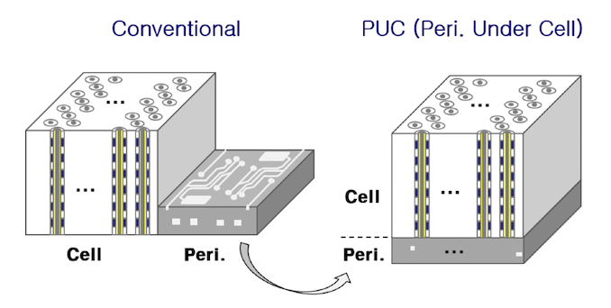
SK hynix’s NAND decks continue to be built with their charge-trap, CMOS under Array (CuA) architecture, which sees the bulk of the NAND’s logic placed under the NAND memory cells. According to the company, their initial 512Gbit TLC part has a die size of 35.58mm2, which works out to a density of roughly 14.39 Gbit/mm2. That’s a 35% improvement in density over their previous-generation 176L TLC NAND die at equivalent capacities. Notably, this does mean that SK hynix will be ever so slightly trailing Micron’s 232L NAND despite their total layer count advantage, as Micron claims they’ve hit a density of 14.6 Gbit/mm2 on their 1Tbit dies.
| SK hynix 3D TLC NAND Flash Memory | ||
| 238L | 176L | |
| Layers | 238 | 176 |
| Decks | 2 (x119) | 2 (x88) |
| Die Capacity | 512 Gbit | 512 Gbit |
| Die Size (mm2) | 35.58mm2 | ~47.4mm2 |
| Density (Gbit/mm2) | ~14.39 | 10.8 |
| I/O Speed | 2.4 MT/s (ONFi 5.0) |
1.6 MT/s (ONFI 4.2) |
| CuA / PuC | Yes | Yes |
Speaking of 1Tbit, unlike Micron, SK hynix is not using the density improvements to build higher capacity dies – at least, not yet. While the company has announced that they will be building 1Tbit dies next year using their 238L process, for now they’re holding at 512Gbit, the same capacity as their previous generation. So all other factors held equal, we shouldn’t expect the first wave drives built using 238L NAND to have any greater capacity than the current generation. But, if nothing else, at least SK hynix’s initial 238L dies are quite small – though whether that translates at all to smaller packages remains to be seen.
Besides density improvements, SK hynix has also improved the performance and power consumption of their NAND. Like the other NAND vendors, SK hynix is using this upcoming generation of NAND to introduce ONFi 5.0 support. ONFi 5.0 is notable for not only increasing the top transfer rate to 2400MT/second – a 50% improvement over ONFi 4.2 – but it also introduces a new NV-LPDDR4 signaling method. As it’s based on LPDDR signaling (unlike the DDR3-derrived mode in ONFi 4.x), NV-LPDDR4 offers tangible reductions in the amount of power consumed by NAND signaling. SK hynix isn’t breaking their power consumption figures out to this level of detail, but for overall power consumption, they’re touting a 21% reduction in energy consumed for read operations. Presumably this is per bit, so it will be counterbalanced by the 50% improvement in bandwidth.
This week’s announcement comes as SK hynix has begun shipping samples of the 238L NAND to their customers. As previously mentioned, the company is not planning on kicking off mass production until H1’2023, so it will be some time before we see the new NAND show up in retail products. According to SK hynix, their plan is to start with shipping NAND for consumer SSDs, followed by smartphones and high-capacity server SSDs. That, in turn, will be followed up with the introduction of 1Tbit 238L NAND later in 2023.
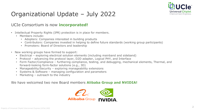
UCIe Consortium Incorporates, Adds NVIDIA and Alibaba As Members
![]()
Among the groups with a presence at this year’s Flash Memory Summit is the UCIe Consortium, the recently formed group responsible for the Universal Chiplet Interconnect Express (UCIe) standard. First unveiled back in March, the UCIe Consortium is looking to establish a universal standard for connecting chiplets in future chip designs, allowing chip builders to mix-and-match chiplets from different companies. At the time of the March announcement, the group was looking for additional members as it prepared to formally incorporate, and for FMS they’re offering a brief update on their progress.
First off, the group has now become officially incorporated. And while this is largely a matter of paperwork for the group, it’s none the less an important step as it properly establishes them as a formal consortium. Among other things, this has allowed the group to launch their work groups for developing future versions of the standard, as well as to offer initial intellectual property rights (IPR) protections for members.
More significant, however, is the makeup of the incorporated UCIe board. While UCIe was initially formed with 10 members – a veritable who’s who of many of the big players in the chip industry – there were a couple of notable absences. The incorporated board, in turn, has picked up two more members who have bowed to the peer (to peer) pressure: NVIDIA and Alibaba.
NVIDIA for its part has already previously announced that it would support UCIe in future products (even if it’s still pushing customers to use NVLink), so their addition to the board is not unexpected. Still, it brings on board what’s essentially the final major chip vendor, firmly establishing support for UCIe across all of the ecosystem’s big players. Meanwhile, like Meta and Google Cloud, Alibaba represents another hyperscaler joining the group, who will presumably be taking full advantage of UCIe in developing chips for their datacenters and cloud computing services.
Overall, according to the Consortium the group is now up to 60 members total. And they are still looking to add more through events like FMS as they roll on towards getting UCIe 1.0 implemented in production chiplets.
Phison and Seagate Announce X1 SSD Platform: U.3 PCIe 4.0 x4 with 128L eTLC

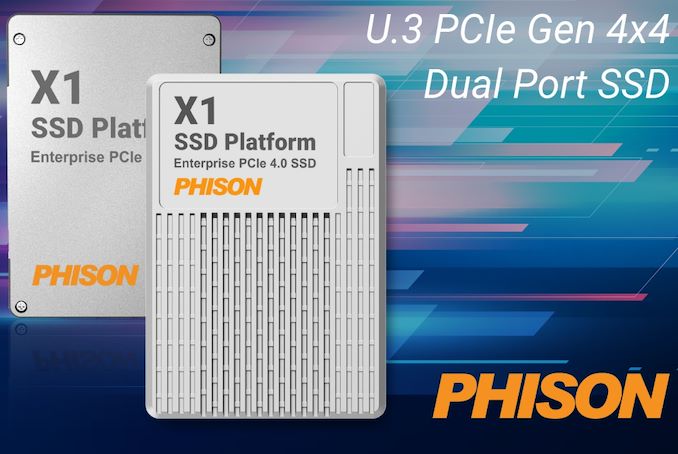
Phison and Seagate have been collaborating on SSDs since 2017 in the client as well as SMB/SME space. In April 2022, they had announced a partnership to develop and distribute enterprise NVMe SSDs. At the Flash Memory Summit this week, the results of the collaboration are being announced in the form of the X1 SSD platform – an U.3 PCIe 4.0 x4 NVMe SSD that is backwards compatible with U.2 slots.
The X1 SSD utilizes a new Phison controller exclusive to Seagate – the E20. It integrates two ARM Cortex-R5 cores along with multiple co-processors that accelerate SSD management tasks. Phison is touting the improvement in random read IOPS (claims of up to 30% faster that the competition in its class) as a key driver for its fit in AI training and application servers servicing thousands of clients. The key specifications of the X1 SSD platform are summarized in the table below. The performance numbers quoted are for the 1DWPD 3.84TB model.
| Seagate / Phison X1 SSD Platform | |
| Capacities | 1.92 TB, 3.84 TB, 7.68 TB, 15.36 TB (1DWPD models) 1.6 TB, 3.2 TB, 6.4 TB, 12.8 TB (3DWPD models) |
| Host Interface | PCIe 4.0 x4 (NVMe 1.4) |
| Form Factor | U.3 (15mm / 7mm z-height) |
| NAND | 128L 3D eTLC |
| Sequential Accesses Performance | 7400 MBps (Reads) 7200 MBps (Writes) |
| Random Accesses Performance | 1.75M IOPS @ QD32T4 & 84us Latency @ QD1 (4K Reads) 470K IOPS @ QD32T4 & 10us Latency @ QD1 (4K Writes) |
| Uncorrectable Bit-Error Rate | 1 in 1018 |
| Power Consumption | 13.5W (Random Reads) 17.9W (Random Writes) 6.5W (Idle) |
Seagate equips the X1 with eTLC (enterprise TLC), power-loss protection capacitors, and includes end-to-end data path protection. SECDED (single error correction / double error detection) and periodic memory scrubbing is done for the internal DRAM as part of the ECC feature. For the contents on the flash itself, the X1 supports the Data Integrity Field / Data Integrity Extension / Protection Information (DIF/DIX/PI) for end-to-end data protection. Various other enterprise-focused features such as SR-IOV support, and NVMe-MI (management interface) are also supported.
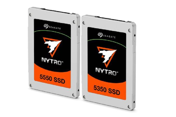
Seagate and Phison claim that the X1 SSD can be customized for specific use-cases, and it offers the best performance in class along with the best energy efficiency. Seagate is marketing the X1 SSD under the Nytro branding – the Nytro 5050 NVMe SSD series for data centers. The Nytro 5350 consists of the 1DWPD models, while the Nytro 5550 makes up the 3DWPD ones.
In terms of competition in the PCIe 4.0 / U.2 / U.3 space, the Nytro 5050 series goes up against Micron’s 7450 PRO and 7450 MAX (PDF), using their 176L 3D TLC flash, and Kioxia’s CD7-V / CD7-R data center SSDs. On paper, Seagate / Phison’s performance specifications easily surpass those platforms that have been shipping for more than a year now.
Compute Express Link (CXL) 3.0 Announced: Doubled Speeds and Flexible Fabrics
While it’s technically still the new kid on the block, the Compute Express Link (CXL) standard for host-to-device connectivity has quickly taken hold in the server market. Designed to offer a rich I/O feature set built on top of the existing PCI-Express standards – most notably cache-coherency between devices – CXL is being prepared for use in everything from better connecting CPUs to accelerators in servers, to being able to attach DRAM and non-volatile storage over what’s physically still a PCIe interface. It’s an ambitious and yet widely-backed roadmap that in three short years has made CXL the de facto advanced device interconnect standard, leading to rivals standards Gen-Z, CCIX, and as of yesterday, OpenCAPI, all dropping out of the race.
And while the CXL Consortium is taking a quick victory lap this week after winning the interconnect wars, there is much more work to be done by the consortium and its members. On the product front the first x86 CPUs with CXL are just barely shipping – largely depending on what you want to call the limbo state that Intel’s Sapphire Ridge chips are in – and on the functionality front, device vendors are asking for more bandwidth and more features than were in the original 1.x releases of CXL. Winning the interconnect wars makes CXL the king of interconnects, but in the process, it means that CXL needs to be able to address some of the more complex use cases that rival standards were being designed for.
To that end, at Flash Memory Summit 2022 this week, the CXL Consortium is at the show to announce the next full version of the CXL standard, CXL 3.0. Following up on the 2.0 standard, which was released at the tail-end of 2020 and introduced features such as memory pooling and CXL switches, CXL 3.0 focuses on major improvements in a couple of critical areas for the interconnect. The first of which is the physical side, where is CXL doubling its per-lane throughput to 64 GT/second. Meanwhile, on the logical side of matters, CXL 3.0 is greatly expanding the logical capabilities of the standard, allowing for complex connection topologies and fabrics, as well as more flexible memory sharing and memory access modes within a group of CXL devices.
Solidigm Announces P41 Plus SSD: Taking Another Shot at QLC With Cache Tiering
Although Intel is no longer directly in the SSD market these days, their SSD team and related technologies continue to live on under the SK hynix umbrella as Solidigm. Since their initial formation at the very end of 2021, Solidigm has been in the process of reestablishing their footing, continuing to sell and support Intel’s previous SSD portfolio while continuing development of their next generation of SSDs. On the enterprise side of matters this recently culminated in the launch of their new D7 SSDs. Meanwhile on the consumer side of matters, today at Flash Memory Summit the company is announcing their first post-Intel consumer SSD, the Solidigm P41 Plus
The P41 Plus is, at a high level, the successor to Intel’s 670p SSD, the company’s second-generation QLC-based SSD. And based on that description alone, a third generation QLC drive from Solidigm is something that few AnandTech readers would find remarkable. QLC makes for cheap high(ish) capacity SSDs, which OEMs love, while computing enthusiasts are decidedly less enthusiastic about them.
But then the P41 Plus isn’t just a traditional QLC drive.
One of the more interesting ventures out of Intel’s time as a client SSD manufacturer was the company’s forays into cache tiering. Whether it was using flash memory as a hard drive cache, using 3D XPoint as a hard drive cache, or even using 3D XPoint as a flash memory cache, Intel tried several ways to speed up the performance of slower storage devices in a cost-effective manner. And while Intel’s specific solutions never really caught on, Intel’s core belief that some kind of caching is necessary proved correct, as all modern TLC and QLC SSDs come with pseudo-SLC caches for improved burst write performance.
While they are divorced from Intel these days, Solidigm is picking up right where Intel left off, continuing to experiment with cache tiering. Coming from the same group that developed Intel’s mixed 3D XPoint/QLC drives such as the Optane Memory H20, Solidigm no longer has access to Intel’s 3D XPoint memory (and soon, neither will Intel). But they do have access to flash memory. So for their first solo consumer drive as a stand-alone subsidiary, Solidigm is taking a fresh stab at cache tiering, expanding the role of the pSLC cache to serve as both a write cache and a read cache.